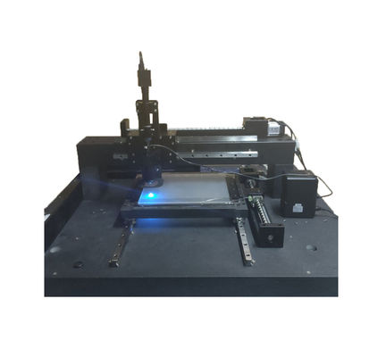
Semiconductor Material Surface Defect Detector
Applications
For the process control and yield management of blank mask in the fields of semiconductor display and
integrated circuit chip manufacturing, we use high throughput optical testing technologies to make fast and
accurate automatic detection for the surface defects of blank mask. According to professional user needs,
we have developed series of high throughput MASK inspection machines with reliable quality and high cost
performance ratio, to help glass substrate, mask and panel manufacturers to identify and monitor the mask
defects, reduce the risk of yield and improve their independent ability of R&D for core technologies.
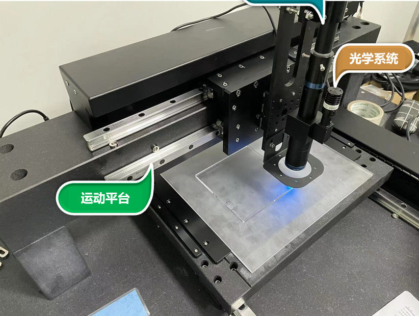
Working Principle
With regards to level and type of surface defect, 4x telecentric lens, specific angle ring light and coaxial light
source are selected as the visual approach. When the device is running, the sample moves along the X
direction and the vision module carries out defect detection along the Y direction.
Features
| Model | SDD0.5-0.5 | |
|
Performance detection |
Detectable defect type | Scratches, Dusts |
| Detectable defect size | 1μm | |
|
Detection accuracy (measured) |
100% detection of defects / collection of defects (scratches, dust) |
|
| Detection efficiency |
≤10 minutes ( Measured value : 350mm x 300mm Mask) |
|
|
Optical System Performance |
Resolution | 1.8μm |
| Magnification | 40x | |
| Visual field | 0.5mm x 0.5mm | |
| Blue light illumination | 460nm,2.5w | |
|
Motion Platform Performance
|
X, Y two-axis motion Marble countertop flatness: 2.5μm Y-axis Z-direction runout precision: ≤ 10.5μm Y-axis Z-direction runout precision: ≤8.5μm
|
|
| Note: Customized production available. | ||
Detection Images
![]()
Our Advantages
We are manufacturer.
Mature process.
Reply within 24 working hours.
Our ISO Certification
![]()
Parts Of Our Patents
![]()
![]()
Parts Of Our Awards and Qualifications of R&D
![]()
![]()
Our products are sold all over the world, you can rest assured.