
Surface Defect Detector in Semiconductor Industry
Applications
For the process control and yield management of blank mask in the fields of semiconductor display manufacturing,
we can help glass substrate, mask and panel manufacturers to identify and monitor the mask defects, reduce the
risk of yield and improve their independent ability of R&D for core technologies.
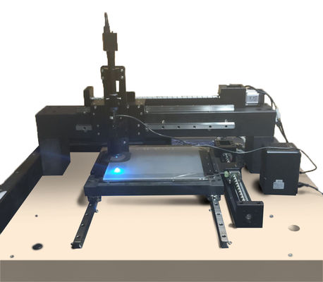
Working Principle
Realize automatic testing of the defects on the mask surface by super-resolution microscopic imaging and super-
resolution defect detection algorithm.
Features
| Model | SDD-S-X—X | |
|
Performance detection |
Detectable defect type | Scratches, Dusts |
| Detectable defect size | 1μm | |
| Detection accuracy (measured) |
100% detection of defects / collection of defects (scratches, dust) |
|
| Detection efficiency |
≤10 minutes ( Measured value : 350mm x 300mm Mask) |
|
|
Optical System Performance |
Resolution | 1.8μm |
| Magnification | 40x | |
| Field of view | 0.5mm x 0.5mm | |
| Blue light illumination | 460nm, 2.5w | |
|
Motion Platform Performance
|
X, Y two-axis motion Marble countertop flatness: 2.5μm Y-axis Z-direction runout precision: ≤ 10.5μm Y-axis Z-direction runout precision: ≤8.5μm |
|
| Note: Customized production available. | ||
Detection Images
![]()
Our Advantages
We are manufacturer.
Mature process.
Reply within 24 working hours.
Our ISO Certification
![]()
Parts Of Our Patents
![]()
![]()
Parts Of Our Awards and Qualifications of R&D
![]()
![]()
Our products are sold all over the world, you can rest assured.
