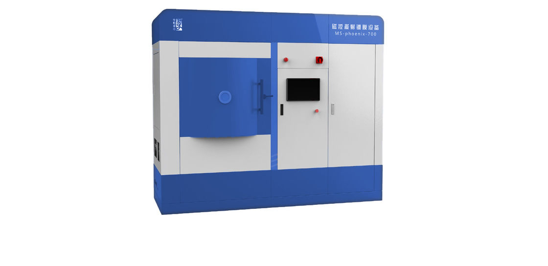

Magnetron Sputtering Deposition in Optics Industry
Applications
| Applications | Specific Purpose | Material Type |
| Optics |
Optical films such as antireflection film, |
SiO2, TiO2, Ta2O5, ZrO2, HfO2 |
| Low-emission glass |
Multiple layers of metal (silver, copper, tin, etc.) |
|
| Transparent conducting glass | ZnO:Al, etc |
Working Principle
The features of magnetron sputtering are high film-forming rate, low substrate temperature, good film adhesion
and realizable large area coating. This technology can be divided into DC magnetron sputtering and RF magnetron
sputtering.
Features
| Model | MSC-O-X—X |
| Coating type | Various dielectric films such as metal film, metal oxide and AIN |
| Coating temperature range | Normal temperature to 500℃ |
| Coating vacuum chamber size | 700mm*750mm*700mm (Customizable) |
| Background vacuum | < 5×10⁻⁷mbar |
| Coating thickness | ≥ 10nm |
| Thickness control precision | ≤ ±3% |
| Maximum coating size | ≥ 100mm (Customizable) |
| Film thickness uniformity | ≤ ±0.5% |
| Substrate carrier | With planetary rotation mechanism |
| Target material | 4×4 inches(compatible with 4 inches and below) |
| Power supply | The power supplies such as DC, pulse, RF, IF and bias are optional |
| Process gas | Ar, N2, O2 |
| Note: Customized production available. | |
Coating Sample
![]()
Process Steps
→ Place the substrate for coating into the vacuum chamber;
→ Vacuumize the vacuum chamber at high and low temperature, and rotate the substrate synchronously;
→ Start coating: the substrate is contacted with precursor in sequence and without simultaneous reaction;
→ Purge it with high-purity nitrogen gas after each reaction;
→ Stop rotating the substrate after the film thickness is up to standard and the operation of purging and cooling is
completed, then take out the substrate after the vacuum breaking conditions are met.
Our Advantages
We are manufacturer.
Mature process.
Reply within 24 working hours.
Our ISO Certification
![]()
Parts Of Our Patents
![]()
![]()
Parts Of Our Awards and Qualifications of R&D
![]()
![]()
Our products are sold all over the world, you can rest assured.