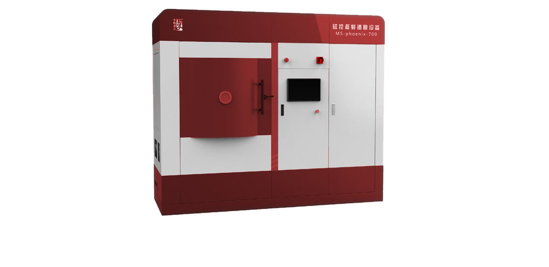

Magnetron Sputtering Deposition in Semiconductor Industry
Applications
| Applications | Specific Purpose | Material Type |
| Semiconductor | IC, LSI electrode, wiring film | AI, Al-Si, Al-Si-Cu, Cu, Au, Pt, Pd, Ag |
| VLSI memory electrode | Mo, W, Ti | |
| Diffusion barrier film | MoSix, Wsix, TaSix,, TiSx, W, Mo, W-Ti | |
| Adhesive film | PZT(Pb-ZrO2-Ti) , Ti, W |
Working Principle
Magnetron sputtering principle: under the action of electric field, electrons collide with argon atoms in the process
of flying to the substrate at a high speed, ionizing plenty of argon ions and electrons, and then electrons fly to the
substrate. Argon ions bombard the target at a high speed under the action of electric field, sputtering lots of target
atoms,then the neutral target atoms (or molecules) deposit on the substrate to form films.
Features
| Model | MSC-SEM-X—X |
| Coating type | Various dielectric films such as metal film, metal oxide and AIN |
| Coating temperature range | Normal temperature to 500℃ |
| Coating vacuum chamber size | 700mm*750mm*700mm (Customizable) |
| Background vacuum | < 5×10⁻⁷mbar |
| Coating thickness | ≥ 10nm |
| Thickness control precision | ≤ ±3% |
| Maximum coating size | ≥ 100mm (Customizable) |
| Film thickness uniformity | ≤ ±0.5% |
| Substrate carrier | With planetary rotation mechanism |
| Target material | 4×4 inches(compatible with 4 inches and below) |
| Power supply | The power supplies such as DC, pulse, RF, IF and bias are optional |
| Process gas | Ar, N2, O2 |
| Note: Customized production available. | |
Coating Sample
![]()
Process Steps
→ Place the substrate for coating into the vacuum chamber;
→ Roughly vacuumize;
→ Turn on molecular pump, vacuumize at top speed, then turn on the revolution and rotation;
→ Heating the vacuum chamber until the temperature reaches the target;
→ Implement the constant temperature control;
→ Clean elements;
→ Revolve and back to the origin;
→ Coating film according to process requirements;
→ Lower temperature and stop the pump assembly after coating;
→ Stop working when the automatic operation is finished.
Our Advantages
We are manufacturer.
Mature process.
Reply within 24 working hours.
Our ISO Certification
![]()
Parts Of Our Patents
![]()
![]()
Parts Of Our Awards and Qualifications of R&D
![]()
![]()
Our products are sold all over the world, you can rest assured.