
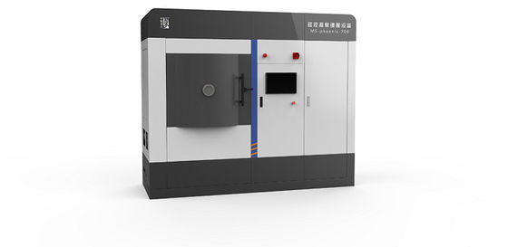
PVD Magnetron Sputtering Deposition
Applications
| Applications | Specific Purpose | Material Type |
| Semiconductor | IC, LSI electrode, wiring film | AI, Al-Si, Al-Si-Cu, Cu, Au, Pt, Pd, Ag |
| VLSI memory electrode | Mo, W, Ti | |
| Diffusion barrier film | MoSix, Wsix, TaSix,, TiSx, W, Mo, W-Ti | |
| Adhesive film | PZT(Pb-ZrO2-Ti) , Ti, W | |
| Display | Transparent conductive film | ITO(In2O; -SnO2) |
| Electrode wiring film | Mo, W, Cr, Ta, Ti, Al, AlTi, AITa | |
| Electroluminescent film |
ZnS-Mn, ZnS-Tb, CaS-Eu, Y2O3, Ta2O5, BaTiO3 |
|
| Magnetic recording | Vertical magnetic recording film | CoCr |
| Film for hard disk | CoCrTa, CoCrPt, CoCrTaPt | |
| Thin film magnetic head | CoTaZr, CoCrZr | |
| Artificial crystal film | CoPt, CoPd | |
| Optical recording | Phase change disc recording film | TeSe, SbSe, TeGeSb, etc |
| Magnetic disk recording film |
TbFeCo, DyFeCo, TbGdFeCo, TbDyFeCo |
|
| Optical disc reflective film | AI, AITi, AlCr, Au, Au alloy | |
| Optical disc protection film | Si3N4, SiO2+ZnS | |
| Perovskite thin-film battery | Transparent conducting layer | ZnO:Al |
| Medical treatment | Biocompatible materials | Al2O3, TiO2 |
| Decorative coating | Colored film, Metallized film | Al2O3, TiO2, and all kinds of metal films |
| Anti-discoloration coating | Precious metal anti-oxidation coating | Al2O3, TiO2 |
| Optical films | High-low refractive index | SiO2, TiO2, Ta2O5, ZrO₂, HfO2 |
| Other applications | Lightproof film | Cr, AlSi, AlTi,etc |
| Resistive film | NiCrSi, CrSi, MoTa, etc | |
| Superconducting film | YbaCuO, BiSrCaCuo | |
| Magnetic film | Fe, Co, Ni, FeMn, FeNi, etc |
Working Principle
Magnetron sputtering is a kind of Physical Vapor Deposition (PVD). It makes the electrons move in spiral
paths near the target surface by the interaction between magnetic and electric fields, thus increasing the
probability of electrons hitting argon gas to generate ions.The generated ions then hit the target surface
under the action of electric field and sputter the target materials to deposite thin film on the substrate surface.
The general sputtering method can be used for preparation of various metals, semiconductors, ferromagnetic
materials, as well as insulated oxides, ceramics and other substances. The equipment uses PLC+ touch
panel HMI control system, which can enter parameters by programmable process interface, with the functions
such as single target sputtering, multi-target sequential sputtering and co-sputtering.
Features
| Model | MSC700-750-700 |
| Coating type | Various dielectric films such as metal film, metal oxide and AIN |
| Coating temperature range | Normal temperature to 500℃ (Customizable) |
| Coating vacuum chamber size | 700mm*750mm*700mm (Customizable) |
| Background vacuum | <5×10⁻⁷mbar |
| Coating thickness | ≥10nm |
| Thickness control precision | ≤±3% |
| Maximum Coating Size | ≥100mm (Customizable) |
| Film thickness uniformity | ≤±0.5% |
| Substrate carrier | With planetary rotation mechanism |
| Target Material | 4x4 inches (compatible with 4 inches and below) |
| Power Supply | The power supplies such as DC, pulse, RF, IF and bias are optional |
| Process Gas | Ar, N2, O2 |
| Note: Customized production available. | |
Coating Sample
![]()
Process Steps
→ Place the substrate for coating into the vacuum chamber;
→ Roughly vacuumize;
→ Turn on molecular pump, vacuumize at top speed, then turn on the revolution and rotation;
→ Heating the vacuum chamber until the temperature reaches the target;
→ Implement the constant temperature control;
→ Clean elements;
→ Revolve and back to the origin;
→ Coating film according to process requirements;
→ Lower temperature and stop the pump assembly after coating;
→ Stop working when the automatic operation is finished.
Our Advantages
We are manufacturer.
Mature process.
Reply within 24 working hours.
Our ISO Certification
![]()
Parts Of Our Patents
![]()
![]()
Parts Of Our Awards
![]()
![]()
Our products are sold all over the world, you can rest assured.
