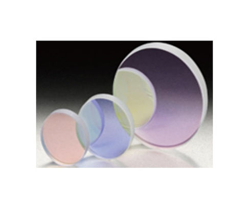
Semi Reflector
Processing Capacity
Capable to realize the complete processes in optical design, instrument design, component high-precision molding,
planar processing, spherical processing, aspheric processing, coating, etc.
Applications
Photoelectric information; aerospace; new energy; nuclear power and nuclear energy equipment and other fields.
Performance
● It is a semi-reflector formed by coating dielectric multilayer film on the surface of parallel substrate or wedge-shaped
substrate.
● A spectroscope divides the incident light into reflected light and transmitted light in a 1:1 ratio.
● The other side is coated with anti-reflection multilayer film.
● It corresponds to a flat semi-reflector with a wide wavelength range.
● The loss of incident light is small because the dielectric film is hardly absorbed. However, the reflectivity and
transmittance vary with the wavelength, polarization state and angle of incidence. The higher the reflectivity,
the greater the variation.
● In case of a parallel substrate, there will be a phenomenon of double image caused by the offset of optical path
and the reverse reflection. A wedge-shaped substrate can prevent double image.
Features
| Semi Reflector | |
| Model | Reflector-SM-X |
| Material |
H-K9L(BK7), Quartz, CaF2 |
| Optical film | Front: Dielectric multilayer film (R:T=1:1) Back: Antireflection multilayer film |
| Surface precision | λ/10 |
| Parallelism | ≤30 seconds |
| Surface quality | 20-10 |
| Dimensional tolerance | ±0.1mm |
| Wavelength for measurement | - |
| Polarization state | No polarization or circular polarization |
Our Advantages
We are manufacturer.
Mature process.
Reply within 24 working hours.
Our ISO Certification
![]()
Parts Of Our Patents
![]()
![]()
Parts Of Our Awards and Qualifications of R&D
![]()
![]()
Our products are sold all over the world, you can rest assured.