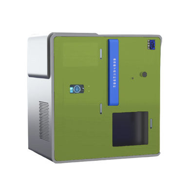

Atomic Layer Deposition in Nanostructure and Pattern Industry
Applications
| Applications | Specific Purpose |
| Nanostructure and pattern |
Template-assisted nanostructure |
| Catalyst-assisted nanostructure | |
| Regioselective ALD for nanopattern preparation |
Working Principle
Atomic layer deposition is a method of forming film by making the gaseous phase precursors pulsed alternately
into the reaction chamber and producing the gas-solid phase chemisorption reaction on the deposited substrate
surface. When the precursors reach the surface of the deposited substrate, they will be chemically adsorbed on
the surface and produce the surface reactions.
Features
| Model | ALD-NP-X—X |
| Coating film system | AL2O3, TiO2, ZnO, etc |
| Coating temperature range | Normal temperature to 500℃ (Customizable) |
| Coating vacuum chamber size |
Inner diameter: 1200mm, Height: 500mm (Customizable) |
| Vacuum chamber structure | According to customer’s requirements |
| Background vacuum | <5×10⁻⁷mbar |
| Coating thickness | ≥0.15nm |
| Thickness control precision | ±0.1nm |
| Coating size | 200×200mm² / 400×400mm² / 1200×1200 mm², etc |
| Film thickness uniformity | ≤±0.5% |
| Precursor and carrier gas |
Trimethylaluminum, titanium tetrachloride, diethyl zinc, pure water, |
| Note: Customized production available. | |
Coating Samples
![]()
![]()
Process Steps
→ Place the substrate for coating into the vacuum chamber;
→ Vacuumize the vacuum chamber at high and low temperature, and rotate the substrate synchronously;
→ Start coating: the substrate is contacted with precursor in sequence and without simultaneous reaction;
→ Purge it with high-purity nitrogen gas after each reaction;
→ Stop rotating the substrate after the film thickness is up to standard and the operation of purging and cooling is
completed, then take out the substrate after the vacuum breaking conditions are met.
Our Advantages
We are manufacturer.
Mature process.
Reply within 24 working hours.
Our ISO Certification
![]()
Parts Of Our Patents
![]()
![]()
Parts Of Our Awards and Qualifications of R&D
![]()
![]()