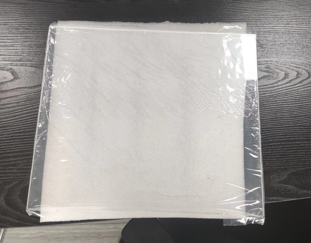
350mm × 300mm Quartz Photomask Substrate For FPD Use
Applications
The fields of photolithography process, such as integrated circuit chip manufacturing, FPD (Flat Panel Display),
MEMS (Micro Electro Mechanical Systems), etc.
Working Principle
Mask is a graphic master mask commonly used in photolithography of micro-nano fabrication. The graphic structure
is formed on a transparent substrate by an opaque photomask, and then the graphic information is transferred to the
product substrate through an exposure process.
Features
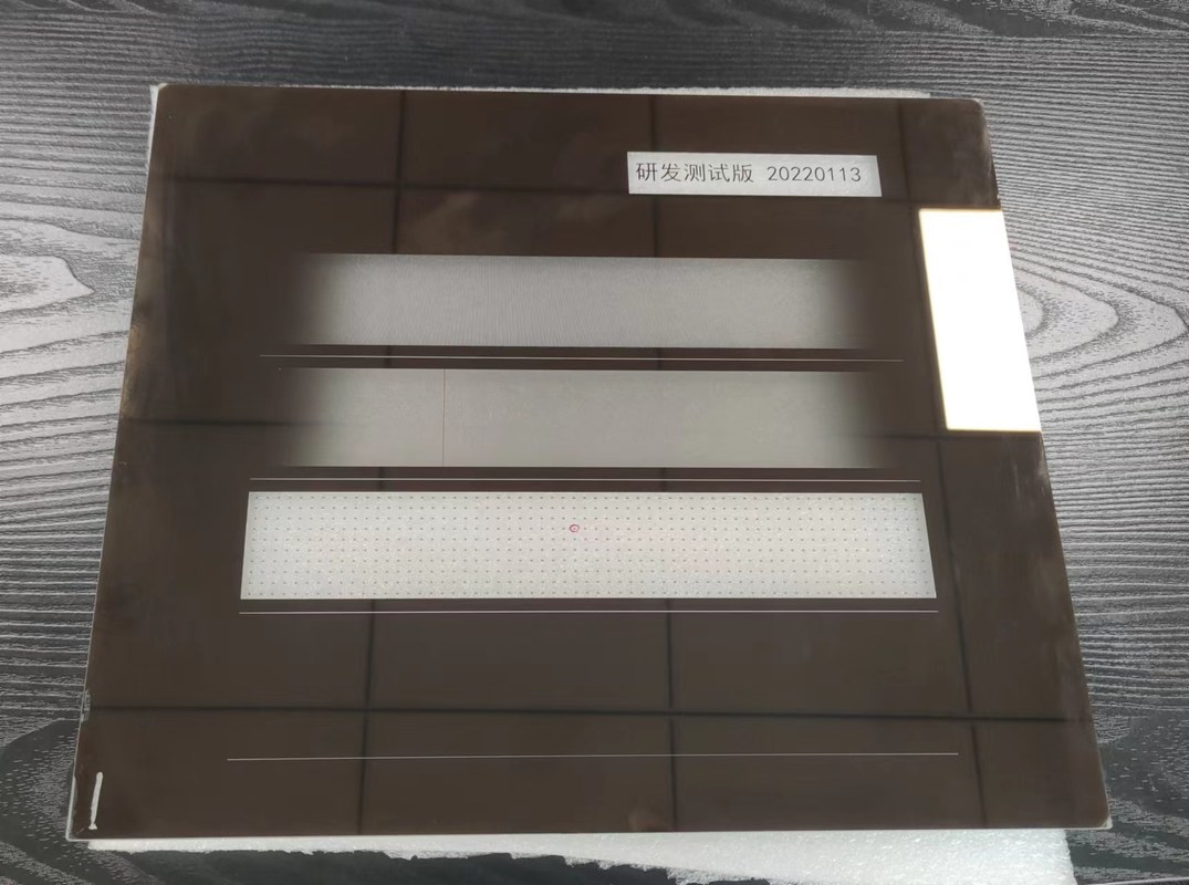
Photomask Substrate for FPD use
| Model / Material | Size | Processing Capacity |
| 3035 / Quartz | 350mm × 300mm | Grinding, Polishing, Chrome Plating, Gluing |
Process Flow
→ Raw materials detection;
→ Rough grinding;
→ Rough polishing;
→ Mask cleaning;
→ Raw materials performance inspection;
→ Plated by chrome;
→ Mask performance testing;
→ Photoresist coating;
→ Packaging;
→ Transporting.
Our Advantages
We are manufacturer.
Mature process.
Reply within 24 working hours.
Our ISO Certification
![]()
Parts Of Our Patents
![]()
![]()
Parts Of Our Awards and Qualifications of R&D
![]()
![]()
Our products are sold all over the world, you can rest assured.